In this article we present a detailed description of the new APU from AMD, whose code name is Llano. We will unveil the details of the system architecture and of the various components integrated into the chip. We will perform also a comparison with the previous architecture, comparing an A8-3850 with a Phenom II x4 840 and a Phenom II 945.
Overview
The Lynx platform is the platform designated by AMD for the mainstream desktop market.
The target audience are the low-power desktop, like the HTPC, All-in-One desktop and dedicated desktop systems for office use, casual gaming and browsing.
The key component is the Llano APU.
After showing the performance and features of the Lynx platform and in particular of the A8-3850 CPU (VERSIONE ITALIANA), in the following pages we will perform a thorough analysis of the architecture and components of the Llano APU, starting with the CPU cores that compose it, including a performance comparison against the previous Stars architecutre, namely Propus and Deneb, concluding with an analysis of the integrated GPU and Northbridge.
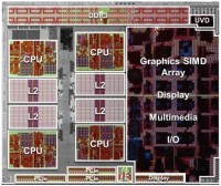
In the first picture you can see a simplified block diagram of the Llano chip. In the second picture you can see a photo of the Llano die.
The heart of the APU are a number of CPU cores, each with its own L1 and L2 caches.
Equally important is the GPU, of DirectX11 class, with an adjacent third-generation UVD unit.
As for external connections we have a memory controller (MC) capable of supporting dual channel DDR3 with 1866 transfers per second, 64 bits each, and the GIO module, which includes the PCI Express 2.0 bus of 24 lines for the connection of both an additional video card or additional displays, both for the implementation of the Unified Media Interface to connect to the Fusion Controller Hub (FCH), and to implement 4 PCI Express link, to avoid encumbering the FCH, and finally the HDMI, DVI and Display Port video links.
The switching center of all data is the north bridge (NB), which is responsible for traffic routing between all the components mentioned above.
The icing on the cake is TurboCore 2.0 technology, which performs a dynamic overclocking of the CPU (and in future architectures also of the GPU), depending on the actual workload of each element.
- Indietro
- Avanti >>


